

Omicron NanoSAM
SEM
Name (abbreviation) of the procedure: Scanning electron microscopy (SEM)
Generic term of the process: SE, BSE
Physical Principle: Generation of electrons which are scattered from the sample material (BSE, primary electrons) and electrons which are removed from the material (SE, secondary electrons)
Scope: Spatial resolution method.Uses electrons backscattered (BSE) or secondary (SE) for electron micrographs of sample areas. The BSE can have Z-Contrast showing the average order number of the sample compounds or topological contrast.
XPS, ESCA
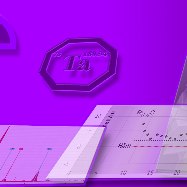
Name (abbreviation) of the procedure: X-Ray photoelectron spectroscopy, Electron spectroscopy for chemical analysis (XPS, ESCA)
Generic term of the process: XPS, ESCA
Physical Principle: Generation of photelectrons via excitation with X-Ray radiation
Scope: Spatial resolution method.Uses an soft X-Ray source to generate photoelectrons to analyze the major and minor compounds. The method is speciation sensitive. Resolution and detection limits inferior to electron probe micro analysis and scanning electron microscopy.
AES
Name (abbreviation) of the procedure: Auger electron spectroscopy (AES)
Generic term of the process: Electron spectroscopy
Physical Principle: Generation of Auger electrons via Excitation with electron gun or X-Ray radiation
Scope: Spatial/surface resolution method, uses low energy electrons or X-Ray source to generate Auger-electrons. The method is speciation sensitive, but inferior to XPS / ESCA

Information
Type: Auger-Sonde
Physical force/principle: X-Ray, Electron
General scope of application: Spatial, Metals, Oxidic, (Surfaces), (Soft matter)
Available at: TU Clausthal
Website: Auger-Nanosonde